[Published in Electronics For You (EFY) magazine, January 2014 edition.] Source
Drawtiming is a free/open source software tool that can be used to generate digital circuit timing diagrams. It is released under the GNU General Public License (GPL). The tool accepts text file as an input from the user and generates image output in different file formats such as PNG, JPEG, PostScript, and PDF. The input needs to adhere to a specific syntax to describe the different signals, their inter-relationships, and transitions as described in the next section with examples.
Before you can try the examples, you need to install the drawtiming tool in your GNU/Linux system. Installation steps may be different from system to system. To install this software in Ubuntu 12.10, just click on Ubuntu Software Centre option from desktop and search for Drawtiming to install it.
For a basic input command example to generate a clock for three periods, the syntax is written as:
CLOCK=0.
CLOCK=1.
CLOCK=0.
A period (.) is used to mark the end of each clock cycle. The first clock period lists and sets the inital states of the signals. Save the above three-line syntax as a .txt file. Here, we name the file as ‘basic.txt’ and save it in a folder named as, say, EFYdraw. Note that the syntax is case sensitive. To generate the timing diagram, open EFYdraw from the terminal window using ‘cd’ command and enter the following command against the prompt, and you will get the output diagram as shown in Fig. 1.
$ drawtiming -o basic.jpg basic.txt
Figure 1.
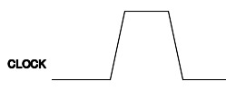
The tick keyword can also indicate a clock cycle. The following syntax creates a single period clock as shown below:
CLOCK=tick.The output diagram is shown in Fig. 2.

Figure 2.
The order in which the signal commands are listed determines the order in which they appear in the output. Multiple signals are separated by commas as shown below:
CLOCK=tick, FLAG=0.The output diagram is shown in Fig. 3.

Figure 3.
A change in one signal that triggers a change in another can be expressed using arrow notation (=>). In the following example (Fig. 4), when the address latch enable (ALE) signal changes state, the read signal (RD) changes its state in the subsequent cycle. The syntax is given below:
ALE=tick,    RD=0.
ALE => RD=1, ALE=0.
Figure 4.
If the transition is in the same clock cycle, it can be indicated in the same clock period. For instance, both CLK and CLK2 change in the second clock period:
CLK=0,    CLK2=0.
CLK=tick, CLK2=1.
The output is shown in Fig. 5.

Figure 5.
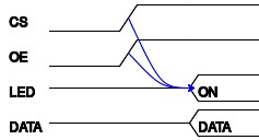
If there are multiple signal changes, you can separate them with a comma. For example, LED is turned on when both the chip select (CS) and output enable (OE) signals change state; then the syntax is written as:
CS=0, OE=0, LED=Z.
CS=1, OE=1.
CS, OE => LED=ON.
The output is as shown in Fig. 6.

Figure 6.
A semicolon can be used to separate a list of dependency signal changes for the same clock period, which is illustrated in the third clock period (refer Fig. 7) in the following example. The syntax is as given below:
CS=0, OE=0, LED=Z, DATA=Z.
CS=1, OE=1.
CS, OE => LED=ON;
DATA=DATA.
Figure 7.
Drawtiming has numerous command line options which can be seen by using the -h option. The supported output image formats are listed in ImageMagick website. A PDF output of the basic.txt example can be created by specifying the .pdf filename extension as shown below:
$ drawtiming -o basic.pdf basic.txtHere, the output will be the same as shown in Fig. 1, only file format is changed to .pdf.
The output image can be scaled with the -x option. To generate an image that is twice the default size, you can use the command as given below:
$ drawtiming -x 2 -o basic-twice.jpg basic.txtThe output is as shown in Fig. 8.

Figure 1.

Figure 8.
If you want to be explicit about the pixel width and height, the -p option followed by width ‘x’ height can be specified as given below:
$ drawtiming -p 250x75 -o basic-p.jpg basic.txtThe output is as shown in Fig. 9.

Figure 1.

Figure 9.
The default cell width and height are 64 and 48 pixels, respectively. The -w and -c options are used to modify them:
$ drawtiming -c 100 -o basic-c.jpg basic.txtThe output is as shown in Fig. 10.

Figure 1.

Figure 10.
The line width can be changed using the -l option. For example:
$ drawtiming -l 3 -o basic-l.jpg basic.txtThe output is as shown in Fig. 11.

Figure 1.

Figure 11.
The default font size is 25 points. You can change it with the -f option. You can also specify a different font using the –font
$ drawtiming -f 10 -o basic-f.jpg basic.txtThe output is as shown in Fig. 12.

Figure 1.

Figure 12.
Timing delays can be displayed in the output using -tD> construct between any two signals. In a simple I/O write cycle, the minimum time between a valid address and the I/O write (IOW) strobe is shown as 92 units (minimum) as follows:
ADDRESS="VALID ADDRESS", DATA="", IOW=1.
DATA="", IOW=0.
ADDRESS -92min> IOW;
DATA="VALID DATA".
IOW=1.
IOW -516min> DATA;
ADDRESS="", DATA="".
The output is as shown in Fig. 13.

Figure 13.
For a real-world example, let us consider the write cycle of a 68008 microprocessor. During the write cycle, the CPU first asserts the read/write (RW) signal for write operation, followed by the address and data signals. The data strobe (DS) signal is then asserted, and the CPU waits for the receiver to acknowledge the same, as indicated by the data transfer acknowledge (DTACK) signal. The syntax for this ‘write’ cycle is as given below:
CLK=0, ADDRESS=Z, AS=1, RW=X, DS=1, DATA=X, DTACK=1.
CLK=1, RW=1, DATA=Z.
CLK=0, ADDRESS="VALID ADDR".
CLK=1, AS=0, RW=0.
CLK=0, DATA="VALID DATA".
CLK=1, DS=0.
CLK=0, DTACK=0.
CLK=1.
CLK=0, AS=1, DS=1, DTACK=1.
CLK=1, ADDRESS="", RW=1, DATA="".
.
The output is as shown in Fig. 14.

Figure 14.
The 68008 read cycle is similar to the write cycle, except that the read signal in RW is asserted, and the DS signal is asserted one clock period earlier as shown below:
CLK=0, ADDRESS=Z, AS=1, RW=X, DS=1, DATA=X, DTACK=1.
CLK=1, RW=1, DATA=Z.
CLK=0, ADDRESS="VALID ADDR".
CLK=1, AS=0, DS=0.
CLK=0.
CLK=1.
CLK=0, DTACK=0.
CLK=1.
CLK=0, AS=1, DS=1, DATA="DATA", DTACK=1.
CLK=1, ADDRESS="", DATA=Z.
.
The output is as shown in Fig. 15.

Figure 15.